California-based research facility Lawrence Livermore National Laboratory (LLNL) will be hosting a dedication ceremony and media tour of its Advanced Manufacturing Laboratory (AML), a state-of-the-art collaborative facility situated in the Livermore Valley Open Campus (LVOC).
The facility, costing $10 million and sized at 14,000 square feet, features advanced 3D printing equipment and is designed to address manufacturing challenges through the merger of LLNL’s science and engineering expertise with academia and industry, leading to the creation of public-private partnerships.
Attending the ceremony are leaders from the National Nuclear Security Administration (NNSA) as well as LLNL leaders, industry partner representatives and Laboratory experts in advanced manufacturing and 3D printing. The ceremony is set to take place on Thursday, Jan. 23 at the High-Performance Computing Innovation Center, Livermore Valley Open Campus.
Additive manufacturing research at LLNL
The LLNL is a federal research facility based in Livermore, California. Founded by the University of California, Berkeley in 1952, the facility was originally a branch of the Lawrence Berkeley National Laboratory, before the Lawrence Livermore laboratory became autonomous in 1971 and was designated a national laboratory in 1981.
Described as “a premier research and development institution for science and technology applied to national security,” LLNL’s main focus surrounds ensuring the safety, security, and reliability of the nation’s nuclear weapons. The facility achieves this through the application of advanced science, engineering, and technology. It is primarily funded by the U.S. Department of Energy (DOE).
The LLNL has exhibited a significant output towards additive manufacturing research. The facility aims to leverage its experience in precision engineering, materials science, and high-performance computing to help advance the field of 3D printing. As such, researchers from the facility have consistently attempted to push the boundaries of the technology.
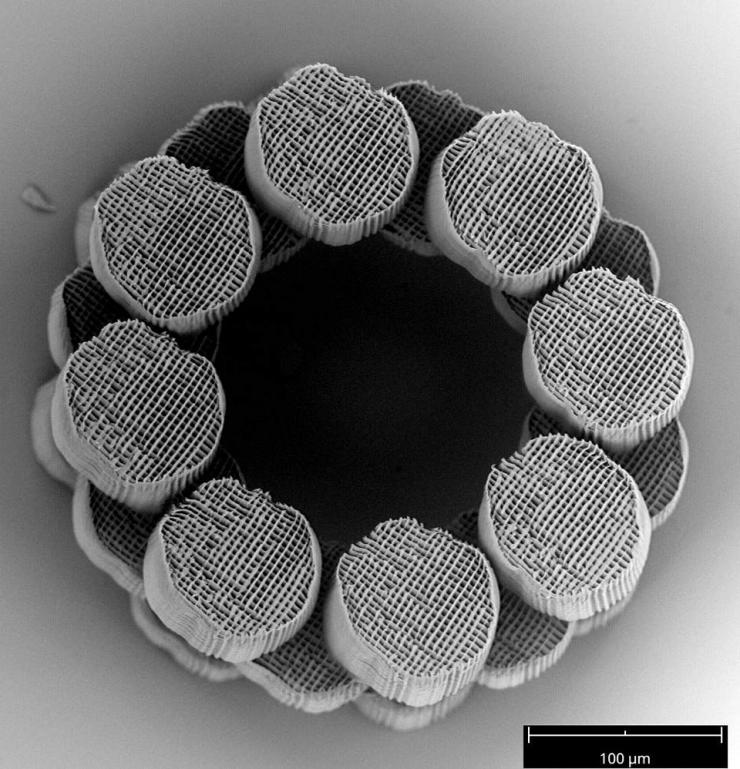
For example, in late 2019, researchers from LLNL, in collaboration with The Chinese University of Hong Kong (CUHK), were able to accelerate the rate of nanoscale additive manufacturing. The team developed a method that could enable industrial-scale production of minute devices. The technique is also capable of creating previously impossible 3D structures with 90-degree overhangs.
Additional research developments from LLNL have included identifying defects in metal 3D printed parts using X-ray imaging, creating a novel bioink capable of creating a substance similar to beer, and 3D printed micro-sized mechanical logic gates, which can enable materials to respond to environmental stimuli.
The new Advanced Manufacturing Laboratory
LLNL’s AML facility is intended to accelerate manufacturing technology through the development of strategic partnerships. Working with its partners, LLNL aims to “reduce production costs and time, while at the same time positively impacting mission-relevant projects in the energy sector, national security and other applications.”
To achieve this goal, the facility will be equipped with advanced additive manufacturing systems, some of which are not yet commercially available. Additional resources include material evaluation and characterization equipment, access to high-performance computing (HPC) modeling and simulation capabilities, and manufacturing systems from several active LLNL research programs. Advances made with the technology at AML are intended to serve dual-purpose applications—both commercial and government products.
Currently, the AML hosts eight industry partners and features a large 5,000-square-foot wet lab for new process development, 3D printing, materials research, chemical work, and other activities. An additional 5,000-square-foot instrument lab will be equipped with metal 3D printing systems and other manufacturing machines, including nanomanufacturing capabilities.
Subscribe to the 3D Printing Industry newsletter for the latest news in additive manufacturing. You can also stay connected by following us on Twitter and liking us on Facebook.
Looking for a career in additive manufacturing? Visit 3D Printing Jobs for a selection of roles in the industry.
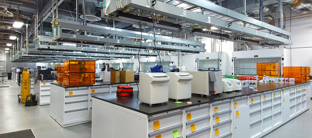
Featured image shows The AML facility. Photo via LLNL.
Leave a comment